
Guide to Pcb production and assembly
Printed Circuit Boards (PCBs) are fundamental components in virtually all electronic devices, from smartphones and computers to industrial machinery and medical equipment. For beginners interested in understanding PCB production and assembly, it is essential to grasp the basic steps involved in transforming a circuit design into a functional PCB. This guide provides an overview of the key stages in PCB production and assembly, including design, fabrication, component placement, and soldering.
The journey of pcb production and assembly begins with the design phase. This stage involves creating a schematic diagram that represents the electrical connections between components. Using Computer-Aided Design (CAD) software, designers convert the schematic into a PCB layout, which outlines the physical placement of components and the routing of electrical traces. The design must consider various factors, such as signal integrity, thermal management, and manufacturability. Once the layout is complete, the design files are exported in a format compatible with manufacturing processes, typically Gerber files.
The next step is PCB fabrication, where the design is transformed into a physical board. Fabrication involves several sub-processes, starting with the preparation of the PCB substrate, usually made of fiberglass-reinforced epoxy laminate (FR-4). The substrate is coated with a thin layer of copper on both sides. The design patterns are then transferred onto the copper using a photolithographic process, where a photosensitive film is exposed to ultraviolet light through a photomask, hardening the exposed areas.
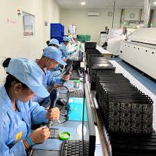
A Beginner’s Guide to Pcb production and assembly
Following the pattern transfer, the PCB undergoes etching to remove unwanted copper, leaving behind the desired circuit traces. The remaining photoresist is stripped away, and the board is cleaned to prepare it for drilling. Drilling is used to create holes for component leads and vias, which connect different layers of the PCB. The drilled holes are then plated with copper to ensure electrical connectivity. Additional layers may be added in multi-layer PCBs, each undergoing similar processes of pattern transfer, etching, and drilling.
Once fabrication is complete, the PCB moves to the assembly stage, where electronic components are mounted onto the board. This process starts with the application of solder paste, a mixture of tiny solder balls and flux, to the PCB pads using a stencil. The components are then placed onto the board, either manually or using automated pick-and-place machines. Surface Mount Technology (SMT) is commonly used for placing small, surface-mount components, while Through-Hole Technology (THT) is used for larger components that require insertion into drilled holes.
After component placement, the board undergoes soldering to secure the components and establish electrical connections. For SMT components, reflow soldering is typically used. The PCB is passed through a reflow oven, where the solder paste melts and solidifies, forming strong joints. For THT components, wave soldering or manual soldering is employed. In wave soldering, the PCB is passed over a wave of molten solder, which adheres to the exposed metal surfaces.
Quality control is a critical part of the PCB production and assembly process. Various inspection techniques, such as Automated Optical Inspection (AOI), X-ray inspection, and functional testing, are used to identify and rectify defects. These tests ensure that the PCB meets design specifications and functions correctly. Once the PCB passes quality control, it is ready for packaging and shipping.
For beginners, understanding PCB production and assembly can seem daunting, but breaking down the process into these stages helps clarify each step. From design and fabrication to assembly and quality control, each phase plays a vital role in producing reliable and efficient PCBs. As technology advances, PCB manufacturing continues to evolve, offering exciting opportunities for innovation and development in electronics. By mastering the basics, beginners can appreciate the complexity and precision involved in creating the backbone of modern electronic devices.