
PCB Board Fabrication
PCB (Printed Circuit Board) fabrication is a vital process in the electronics industry, serving as the foundation for almost all electronic devices. A PCB provides both mechanical support and electrical connections for components such as resistors, capacitors, and microchips. The fabrication process involves several intricate steps to ensure the PCB functions correctly and meets the required specifications. From the initial design phase to the final testing, every aspect of PCB fabrication demands precision and expertise.
The process of PCB fabrication begins with the design phase, where engineers create the layout of the circuit board. This layout is usually designed using specialized software, ensuring that the paths for electrical current flow are optimized. The design is then translated into a blueprint that guides the manufacturing process. A key factor in this stage is the material selection for the PCB. Common materials used in PCB fabrication include FR4 (a fiberglass-based laminate) and CEM1, with each material offering unique properties suited to different applications.
Once the design and material selection are complete, the fabrication process can begin. The first step involves transferring the pcb board fabrication design onto the copper-clad board. This is typically done through a process known as photolithography, where light-sensitive chemicals are used to create patterns on the board. The copper layer is then etched to remove any unwanted copper, leaving behind the necessary electrical traces. These traces will connect various components on the board, allowing the flow of current.
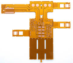
PCB Board Fabrication: An Essential Process in Modern Electronics
After etching, the next step in PCB fabrication is drilling. Holes are drilled into the board to accommodate components that need to be mounted, such as through-hole components. These holes are typically drilled using high-speed rotating tools that precisely penetrate the board. Additionally, vias (small holes that connect different layers of the board) may also be created at this stage for multi-layer PCBs, which are common in complex electronic devices.
Once the drilling is complete, the PCB undergoes a series of processes to ensure proper insulation and durability. This includes the application of a solder mask, which is a layer of polymer applied to protect the copper traces from corrosion and prevent short circuits. The solder mask also ensures that only the areas where components will be soldered remain exposed. Following the solder mask, the PCB is printed with silkscreen to label the components and connections, making it easier to assemble the board.
The final steps in PCB fabrication involve testing and inspection. The board is thoroughly tested to ensure there are no defects in the circuitry, such as open circuits or short circuits. Visual inspection, automated optical inspection (AOI), and electrical testing are all used to verify the board’s integrity and functionality. In addition, each board undergoes a final cleaning process to remove any remaining residues from the fabrication process.
Once the PCB has passed all tests and inspections, it is ready for assembly, where components will be soldered onto the board. The quality of the PCB and the reliability of the end product largely depend on the precision and quality of the fabrication process. Advanced manufacturing technologies such as multi-layer PCBs, flexible PCBs, and HDI (High-Density Interconnect) boards are increasingly being used to meet the demands of modern electronics.
In conclusion, PCB board fabrication is a complex and highly specialized process that requires attention to detail at every step. From design to testing, each stage ensures that the finished PCB is functional, reliable, and ready for use in a wide range of electronic devices. The continuous advancements in PCB technology are helping manufacturers meet the growing demands of modern electronics, making it an exciting field to watch.